
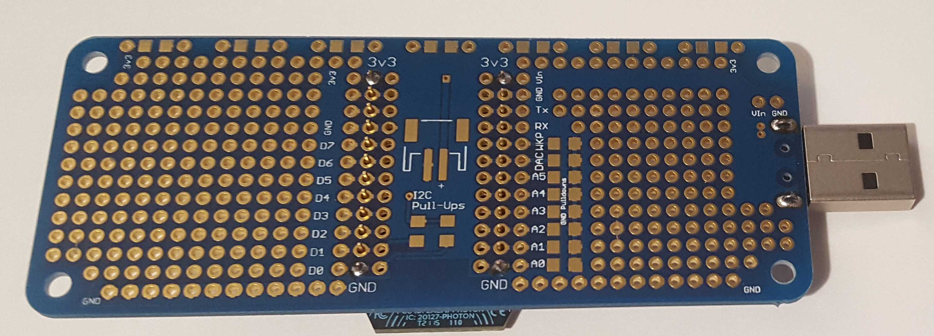
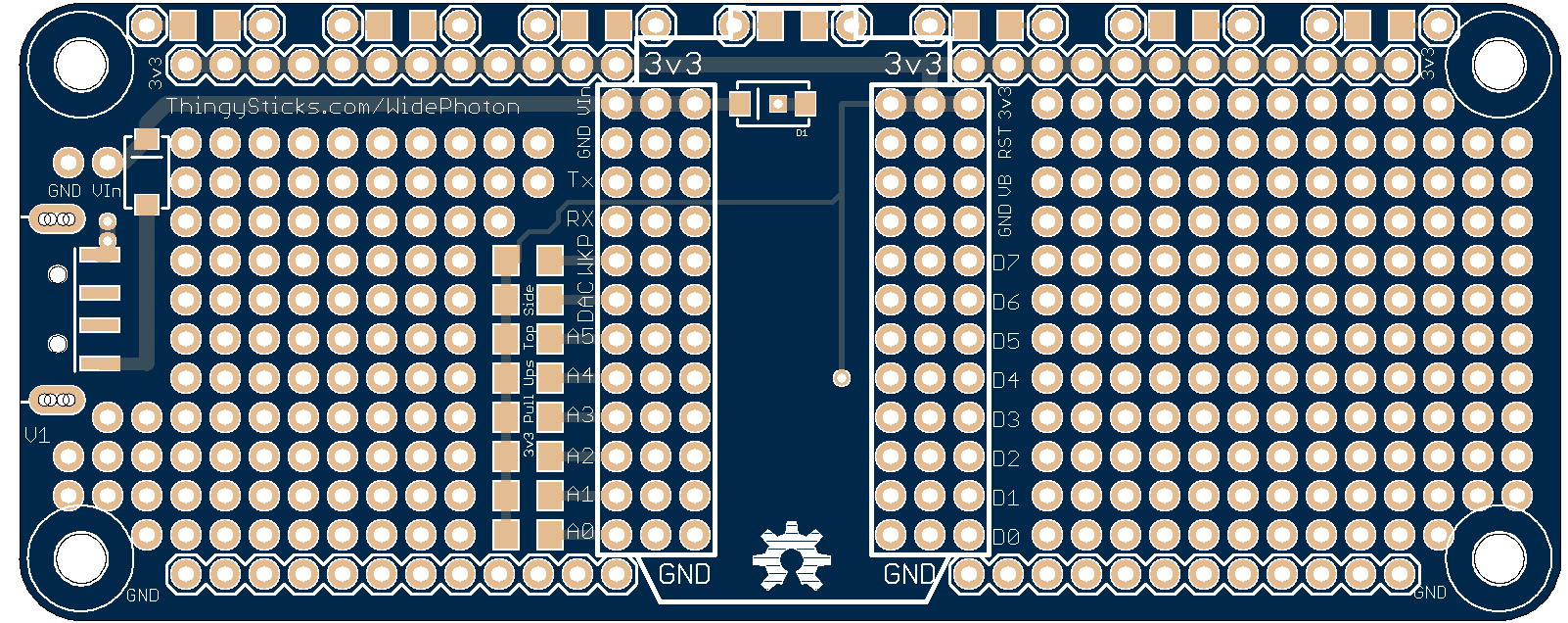


Features
- Wide format, the prototyping area is either side of the Photon making it easier to connect to the GPIO pins on the photon.
- A USB A plug can be mounted onto the PCB allowing the prototype to be plugged directly into a USB power outlet (PC, Wall brick, battery etc.).
- JST socket pads on the PCB bottom allow a standard LiPol battery JST socket to be mounted to power the circuit by a battery or external power supply input.
- Diode protection on the JST and USB A plug prevent current flowing back into the USB or battery when powered by another source.
- The Photons Analog inputs have 3v3 pull-up 1206 pads (PCB top layer) and pull-down 1206 pads (PCB bottom layer) to GND, this makes it easy to create a potential divider on the analog inputs for resistive sensors such as LDRs, thermistors, variable resistors etc.
- 7x 1206 pads top and bottom for SMD LEDs, capacitors, resistors etc along the top edge.
- PCB bottom layer underneath the Photon has 1206 pads connected to D0 and D1 for I2C pull-ups.
- 1206 pads work well of 0804 components as well (they are actually easier to solder).
PCB Layout
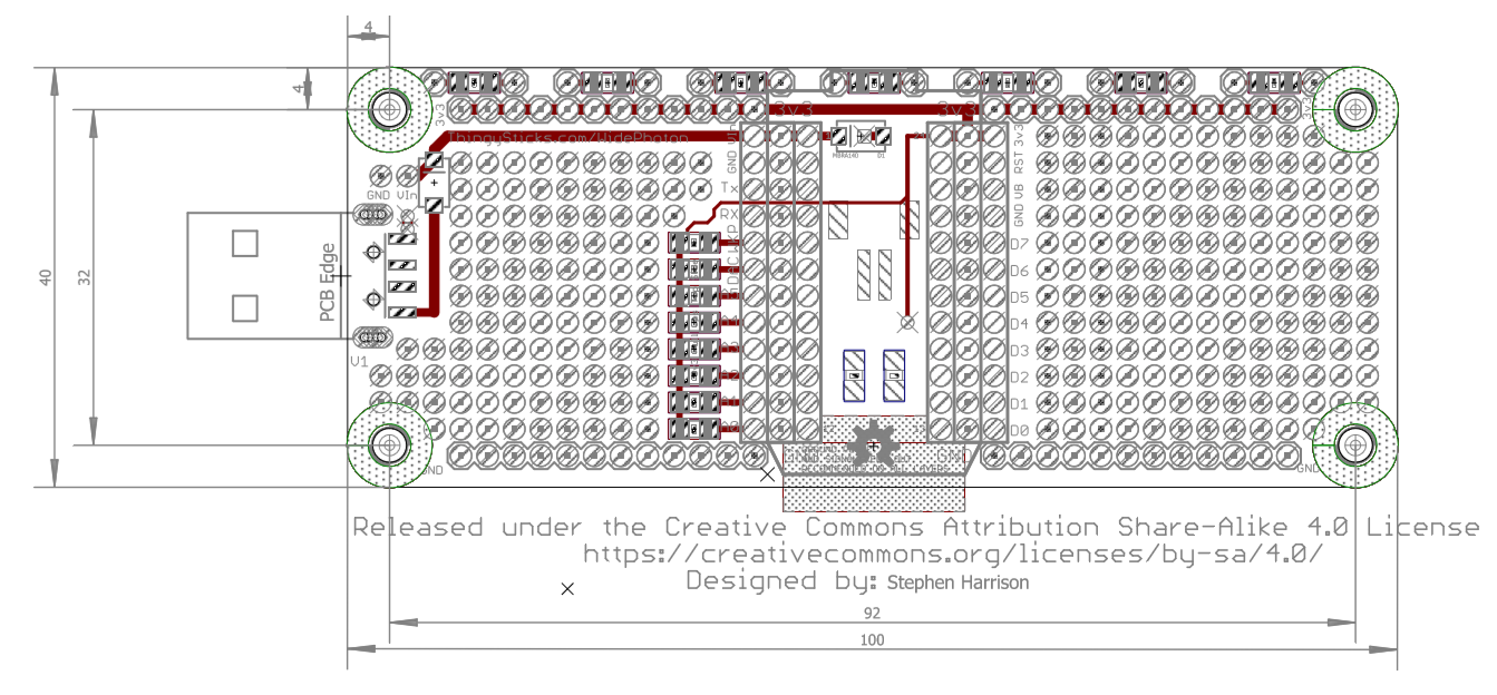
Dimensions
- Length: 100mm
- Width: 40mm
- Hole 1: 3.2mm at 4,4
- Hole 2: 3.2mm at 96,4
- Hole 3: 3.2mm at 4,36
- Hole 4: 3.2mm at 96,36