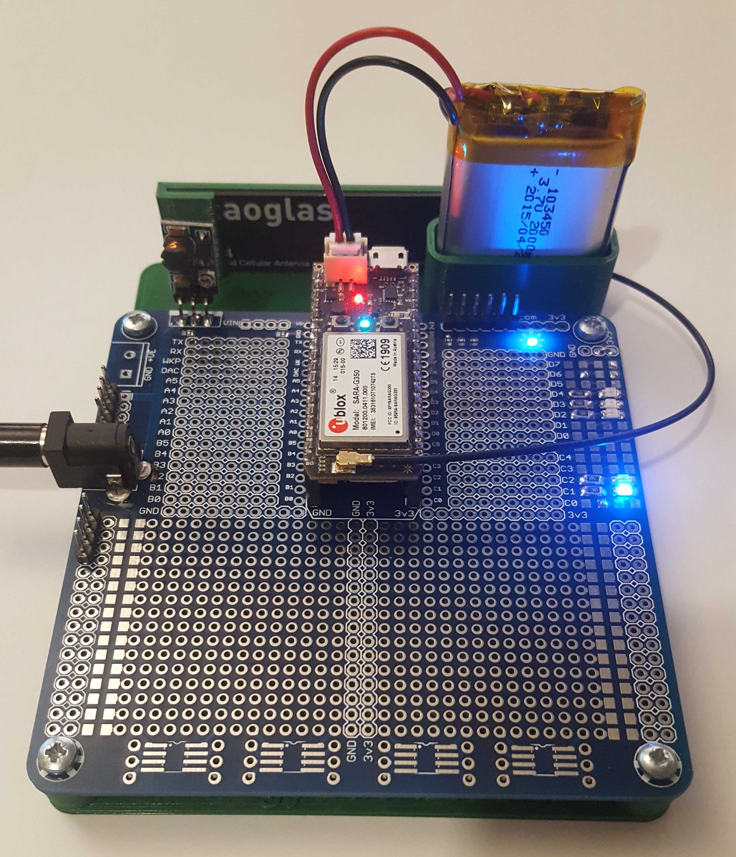
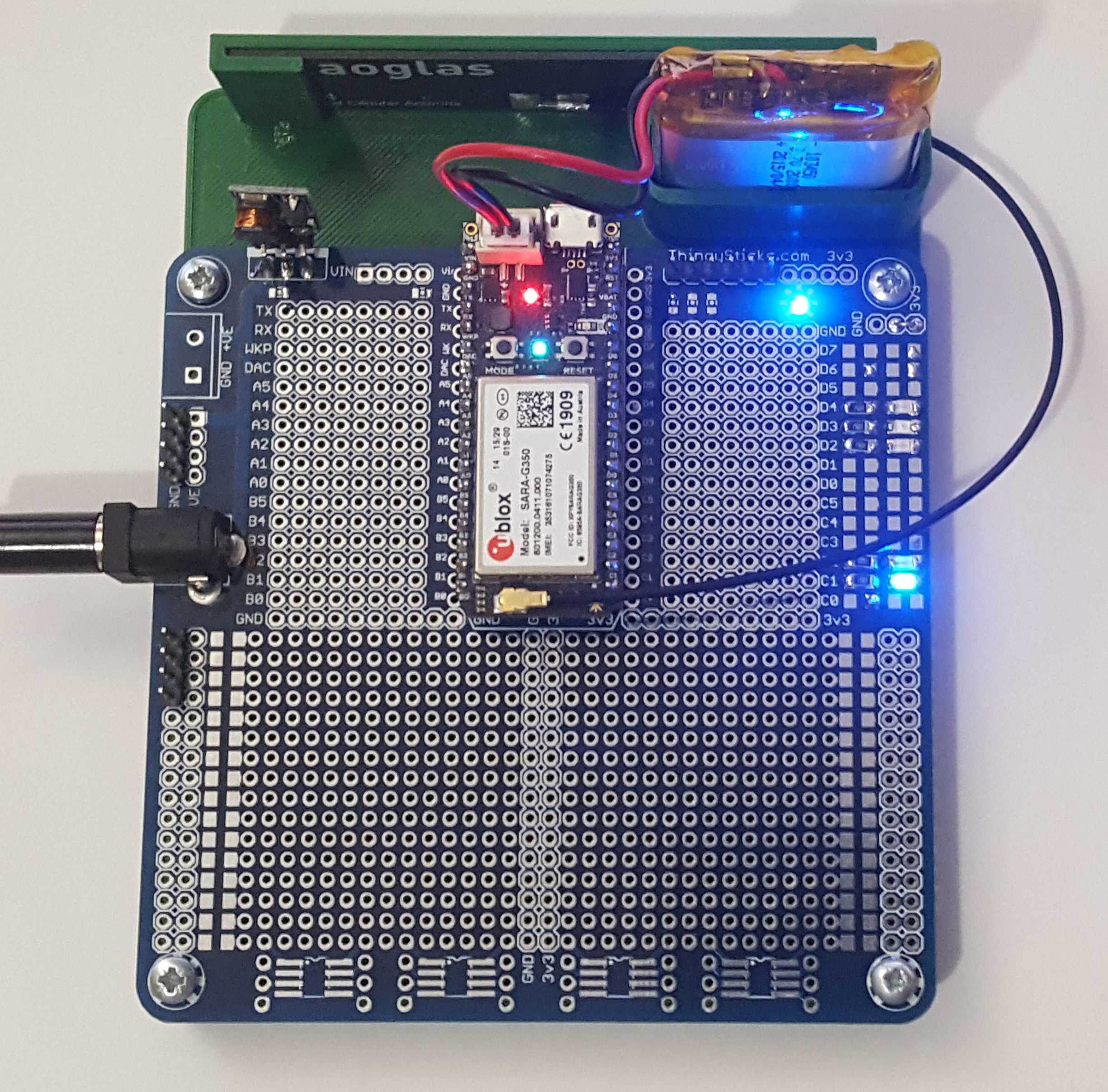
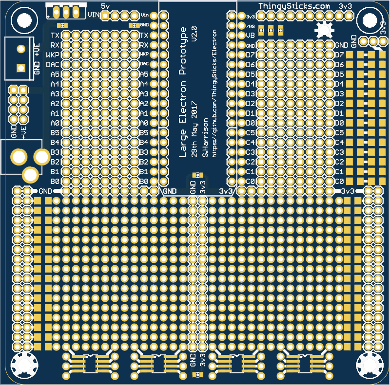
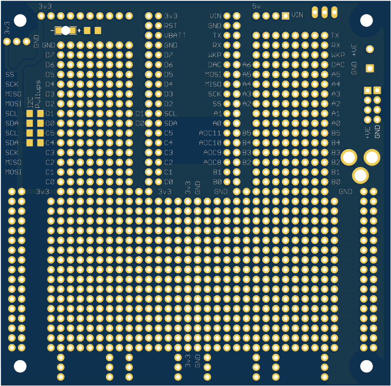
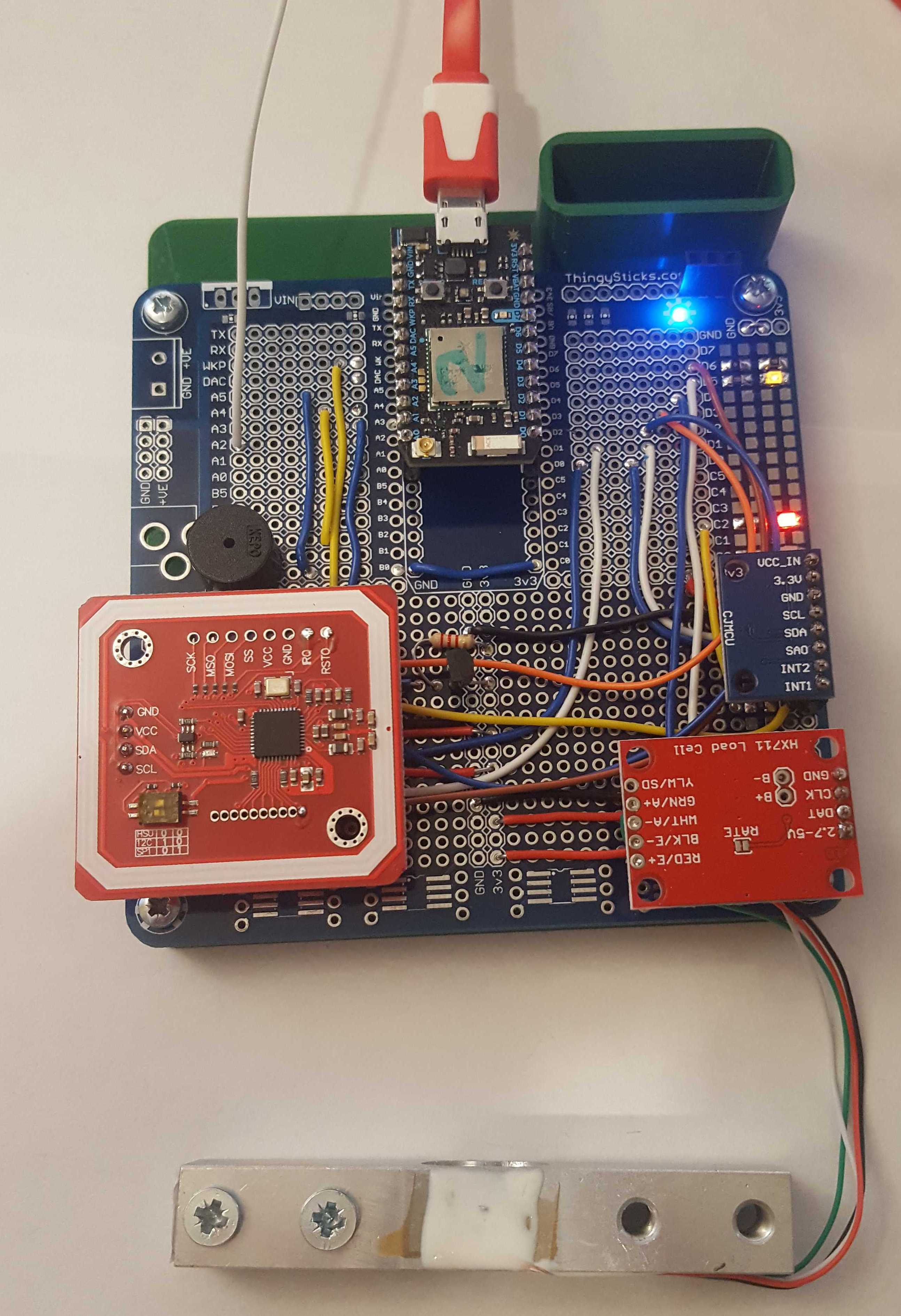
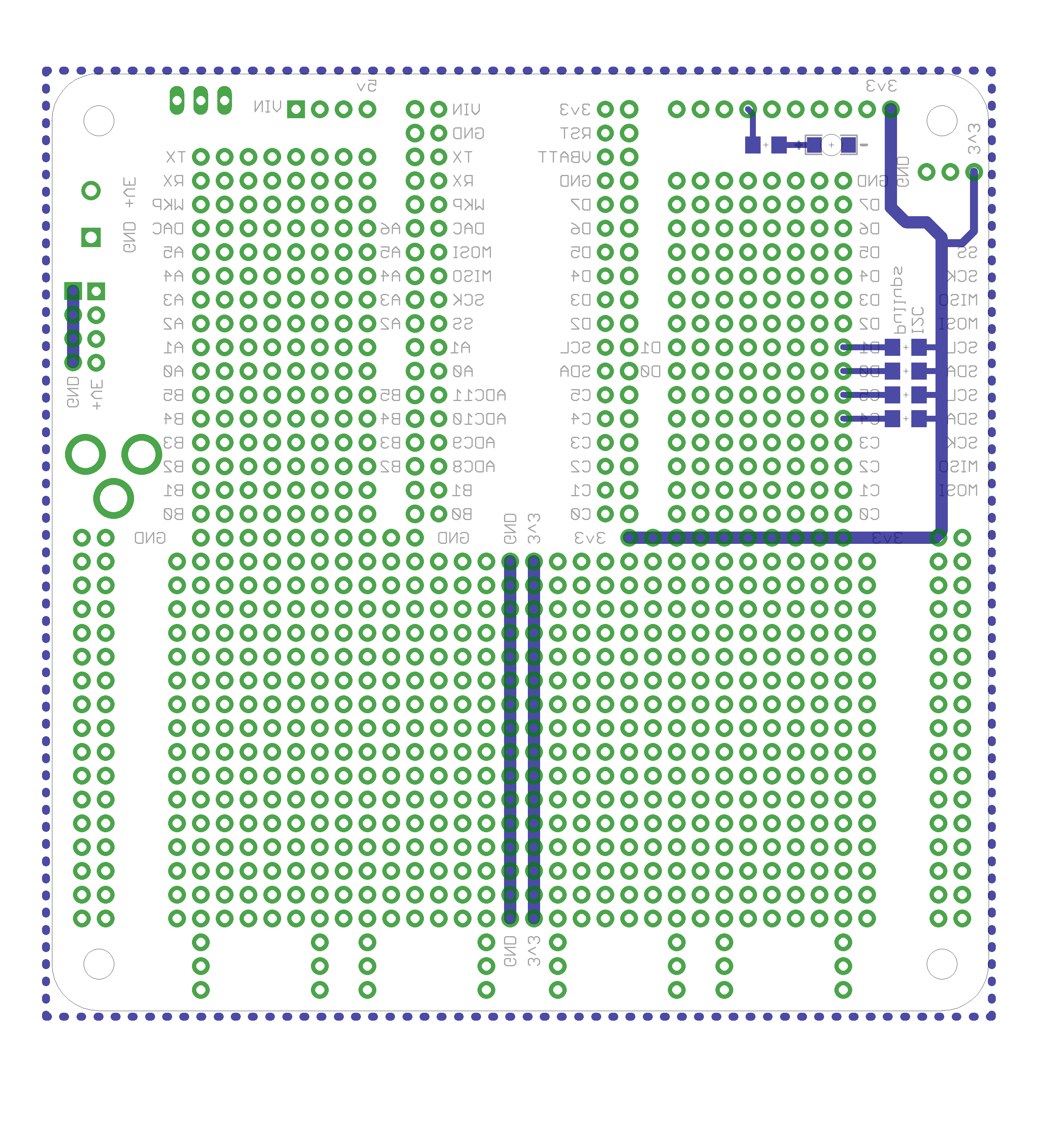
Features
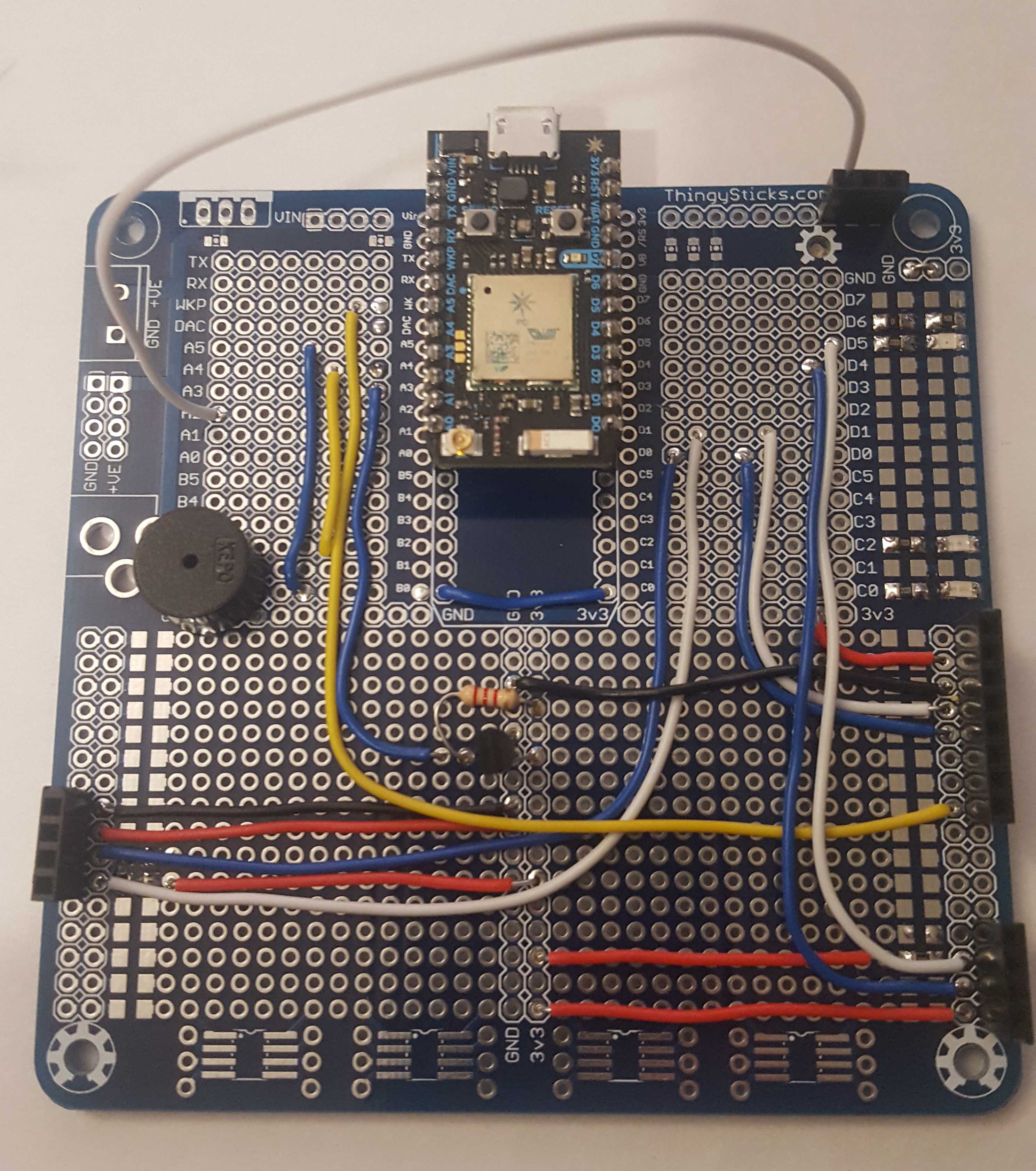
- Large breakout area on the lower half.
- Electron pins connected to breakout pads either side of the device.
- Double 1206 pads for D0-D7 and C0-C5 top side for resistor + led combination, useful for diagnostics on pins.
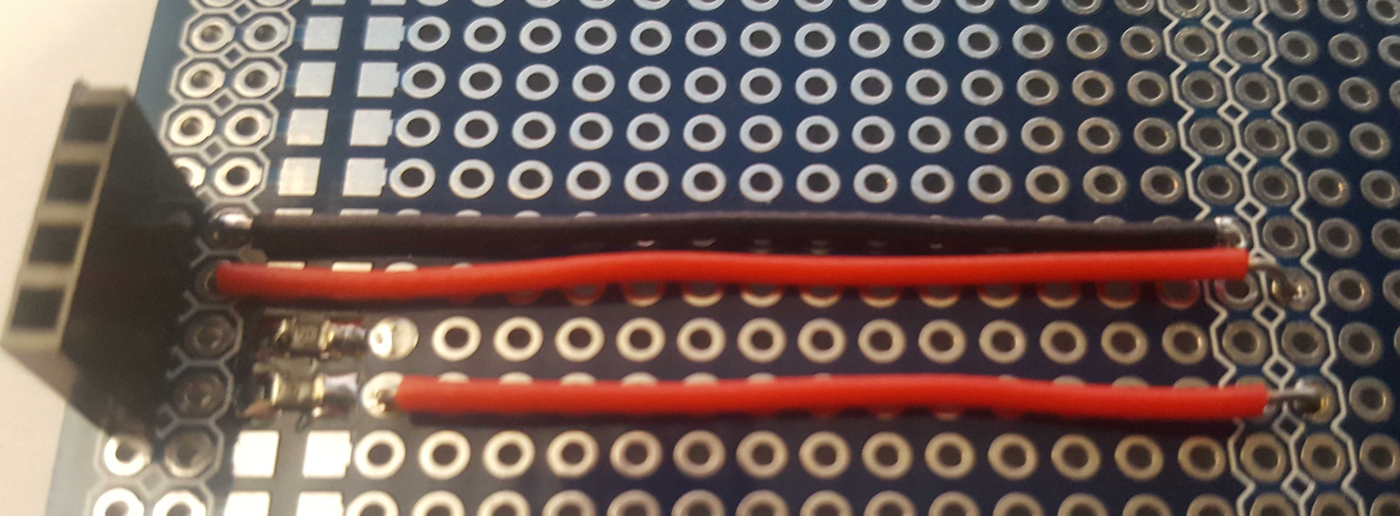
- External connector holes either side of lower half with double collected holes to allow for easy PCB connection to the connector.
- 1206 pads linking external connector pads to internal breakout nearest pad to allow for easy link with resistor.
- 3v3 and GND available down the middle of the breakout area and across the top.
- 4x SOIC08 8 pin SMD pads with connected holes.
- 4x M3 mounting holes.
- Reverse mount LED and resistor pads for 3v3 power light.
- Pads for external power input via DC jack barrel (2.1/2.5mm) or 2 Pin 5mm terminal block and layout for "7805" style buck regulator.
- Excellent Electron pin function PCB silk screen.
- 4x 1206 pads for I2C pullups on D0/D1 and C4/C5 pins.
- Suitable for Photon/Bluz or other Particle pin compatible devices.
PCB Layout
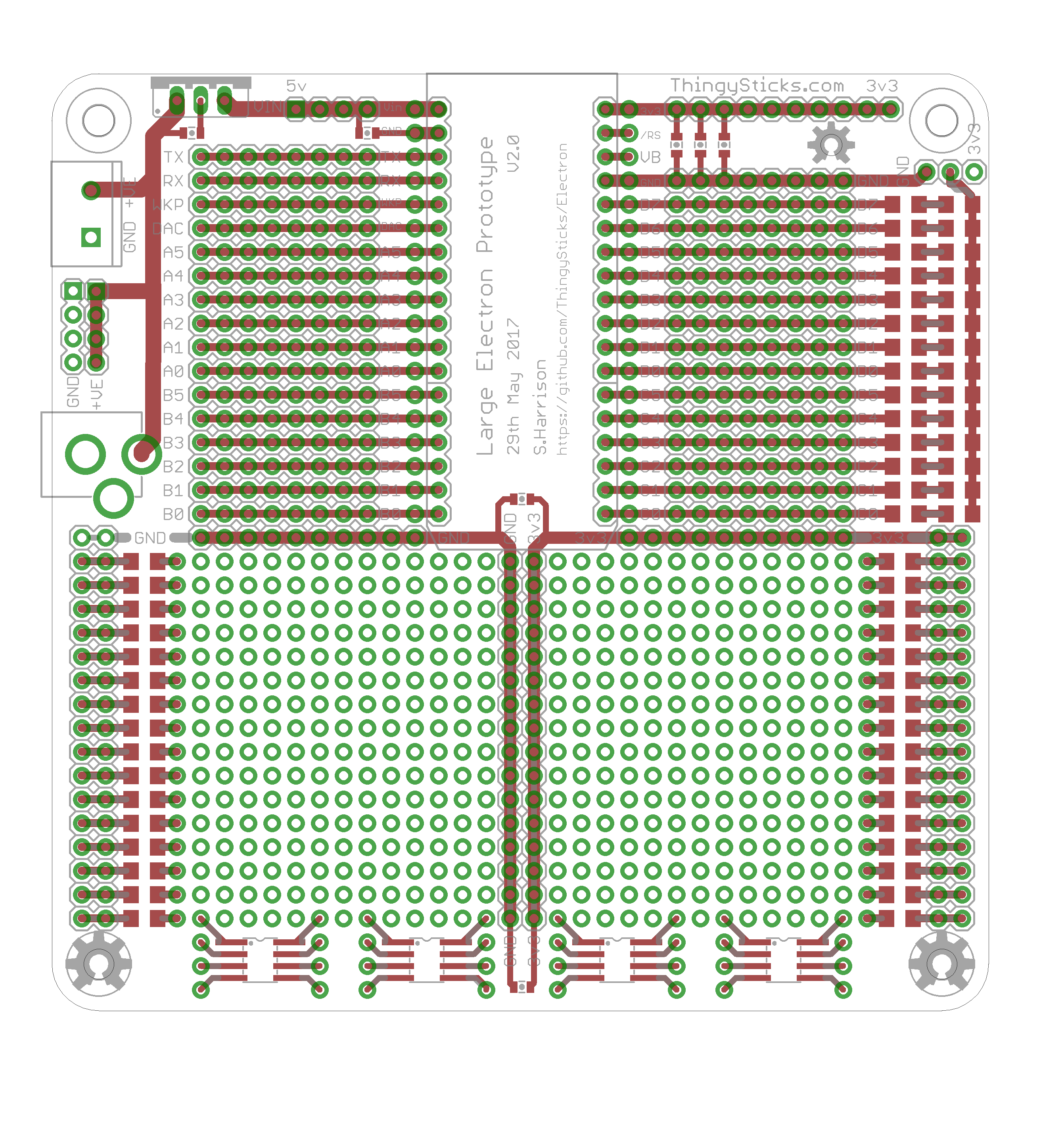
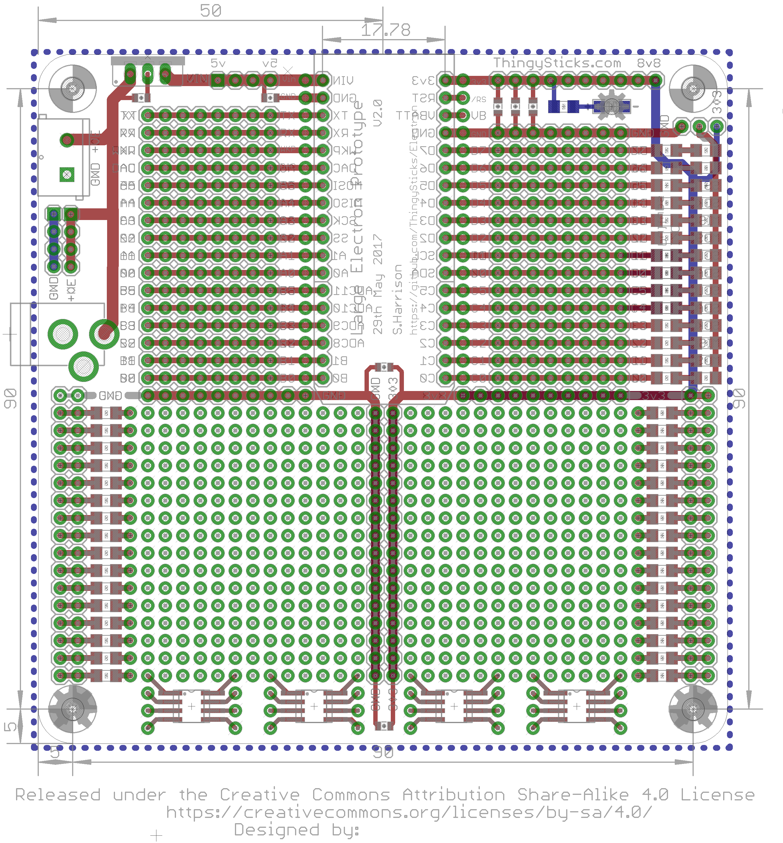
Dimensions
- Length: 100mm
- Width: 100mm
- Hole 1: 3.2mm at 5,5
- Hole 2: 3.2mm at 95,5
- Hole 3: 3.2mm at 95,95
- Hole 4: 3.2mm at 5,95